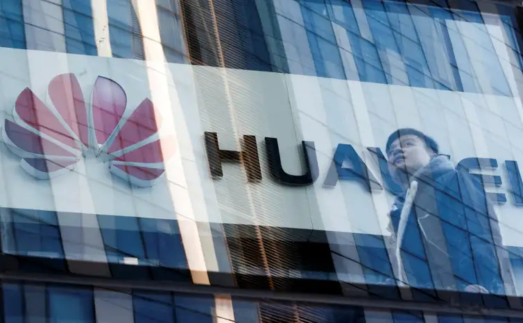
China, unable to access state-of-the-art wafer manufacturing tools from American, European and Japanese manufacturers, needs to develop its own manufacturing equipment. Huawei is building a large research and development (R&D) center near Shanghai, where it plans to develop chipmaking tools that need to be competitive with systems designed by ASML, Canon and Nikon, as reported by Nikkei.
The R&D center will focus on developing lithography machines, which are essential for chip manufacturing at next-generation nodes. Huawei’s partners SMIC and Hua Hong are currently unable to obtain lithography tools that can manufacture logic chips using 14nm/16nm FinFET-based process technologies and higher-end processes, but they can still obtain lithography systems capable of 28nm. Therefore, machines developed by Huawei will have to be at least capable of 28nm, or better yet, 14nm/16nm. ASML currently controls well over 90% of the lithography tool market.
The R&D center is strategically located in Shanghai’s Qingpu District, part of a larger campus that includes facilities for Huawei’s chip design unit, HiSilicon T, as well as R&D centers for wireless technologies and smartphones. The total investment in the campus is estimated at ¥12 billion ($1.66 billion), covering an area equivalent to approximately 224 football fields. Once completed, it will have the capacity to accommodate more than 35,000 employees.
To attract top talent, Huawei is offering competitive salary packages and has already hired engineers with experience at major chip toolmakers and chip manufacturers. Huawei (and other companies based in China) can no longer hire American citizens and US green card holders to lead their projects. Now that ASML, Applied Materials, KLA and Lam Research need to reduce their presence in China, Huawei and other companies in the country can hire experienced talent with Chinese citizenship.
Huawei’s R&D spending reached a record ¥164.7 billion ($22.756 billion) in 2023, accounting for 23.4% of its total revenue. This significant investment highlights the company’s commitment to innovation, and the increase can be attributed to increasing investments in the development of wafer fabrication tools.
Before being added to the US trade blacklist, Huawei mainly focused on chip design, collaborating with large contract chipmakers such as TSMC and GlobalFoundries. However, following restrictions on access to American technologies, the company shifted its focus to working with China-based contract chipmaker SMIC, according to the report. Now, Huawei is reportedly venturing into chip production, entering into partnerships with local government-backed entities in several Chinese cities, including Shenzhen, Qingdao and Quanzhou, which essentially means it invests money in factories operated and co-owned by Huawei. of local and federal governments. Additionally, Huawei has invested in numerous local chip material suppliers in an attempt to use local suppliers and invest in domestic alternatives.
With information from News Agencies.
Source: https://www.ocafezinho.com/2024/06/26/guerra-dos-chips-china-avanca-no-dominio-da-litografia-e-pode-ficar-independente-da-asml/

