China invests billions to create its own machines, while Canon bets on innovation to threaten Asml dominion in the global market
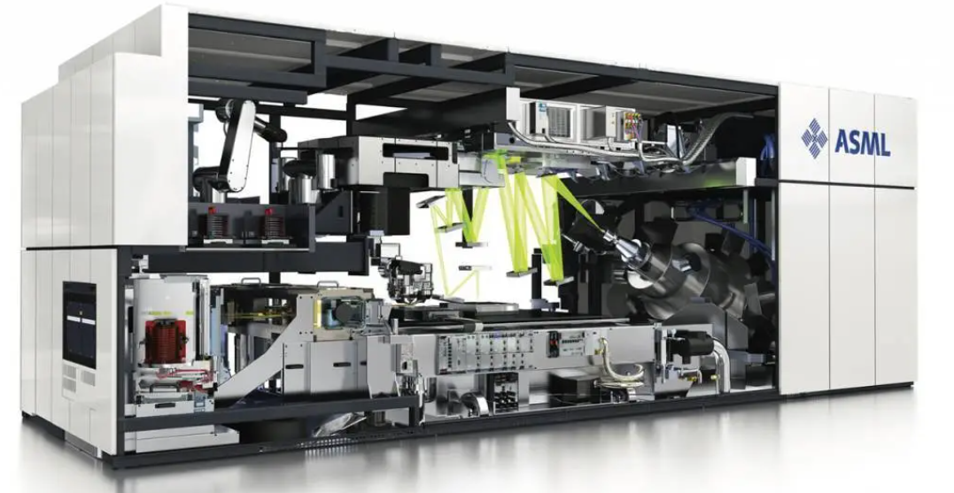
In a quiet Dutch city named Eindhoven, is the headquarters of ASML, a company that became a key piece in the advance of global artificial intelligence (AI). The company is the only extremely advanced lithography machine manufacturer, essential for the production of the most modern AI chips. Its latest creation impresses: a 150 -ton colossal machine, with dimensions equivalent to two containers and valued at about $ 350 million. It is the most sophisticated equipment available on the market today.
According to The Economist magazine, ASML’s expertise put it at the center of global technology disputes. Faced with tensions between US and China, the United States forbade the sale of the company’s most advanced equipment to Chinese manufacturers in an attempt to curb AI chips development in China. In response, the Asian country invests billions to create domestic alternatives.
At the same time, Canon, Japanese rival, bets on a more affordable technology – nanoimpression lithography (Nil) – as a possible alternative to ASML domain. However, unlike the software industry, where leaders can rapidly change, success in lithography demands decades of research and development, making the challenge to ASML hegemony a Herculean task.
The heart of the most advanced ASML machine lies in its capacity to firing 50,000 melted tin droplets inside a vacuum chamber. Each droplet goes through a meticulous process: first, an initial laser the pancake -shaped flat laser; Then a second and powerful bundle completely vaporizes the droplet. The result is a hot plasma that reaches temperatures close to 220,000 ° C – about 40 times warmer than the surface of the sun – and emits extreme ultraviolet light (EUV). This light, reflected by ultra -thin mirrors, is used to print designs on silicon pads covered with light -sensitive chemicals, creating the complex circuits present in modern chips.
ASML tools are indispensable for companies such as TSMC, Samsung and Intel, responsible for the manufacture of advanced processors, from AI accelerators to smartphone chips. No other company can produce machines capable of reliably manufacturing chips classified as “7 nanometers” or smaller, we have today used more as marketing strategies than precise physical references. Even technologies considered older, such as “14nm”, depend strongly on ASML solutions, which dominates over 90% of the market in these segments.
A microchip can be compared to an electronic lasagna: a transistor base covered with intricate copper wire layers that carry data and energy. A modern processor can house more than 100 billion transistors, distributed in more than 70 layers and more than 100 kilometers of wiring, all condensed in a smaller space than a postal seal. To build these tiny components, a lithography machine works in steps, recording patterns that form transistors and layers of metallic wires in a silicon pad, layer layer. A single tablet can contain hundreds of chips.
ASML systems operate based on the principle of old projectors, where light crosses a stencil to design images on a surface. The minimum size of the resources that can be printed depends mainly on two factors: the wavelength of light and the numerical opening of the mirrors. When using EVU light, with 13.5nm wavelength, ASML has drastically reduced the size of chip resources. In addition, their latest systems employ mirrors with high numerical openings, allowing the precise impression of resources as small as 8NM. However, increasing this capacity further requires more advanced and expensive technologies, such as the hyper-na concept, which faces challenges related to energy consumption and astronomical costs.
Meanwhile, China seeks ways to overcome the restrictions imposed by the West. Without access to the most advanced ASML tools, the country explores methods such as multipadronization, which divides a pattern into multiple steps to achieve greater accuracy. SMEE, a Chinese state company, is also developing its own lithography machines, but experts point out that replicating the ASML supply chain – which involves more than 5,000 specialized suppliers – is a monumental challenge.
On the other hand, Canon bets on nanoimpression lithography (Nil) as a viable alternative. Using molds to directly press patterns in the tablets, Nil promises to lower costs and simplify the manufacturing process. However, problems such as defects, precise alignment and limited production rate still make it difficult to adopt on a large scale. While Nil finds space in areas such as smartphone screens and memory chips, it does not yet directly threaten ASML supremacy in the manufacture of state -of -the -art logical chips.
Although ASML’s leadership seems unwavering in the short term, the technological race remains fierce. Future innovations can change the scenario, especially if China gets significant advances or if Canon solves Nil bottlenecks. For now, the most important machine in the world continues to shape the future of computing, AI and technology as a whole.
Source: https://www.ocafezinho.com/2025/03/16/a-maquina-de-us-350-milhoes-que-dita-o-futuro/